
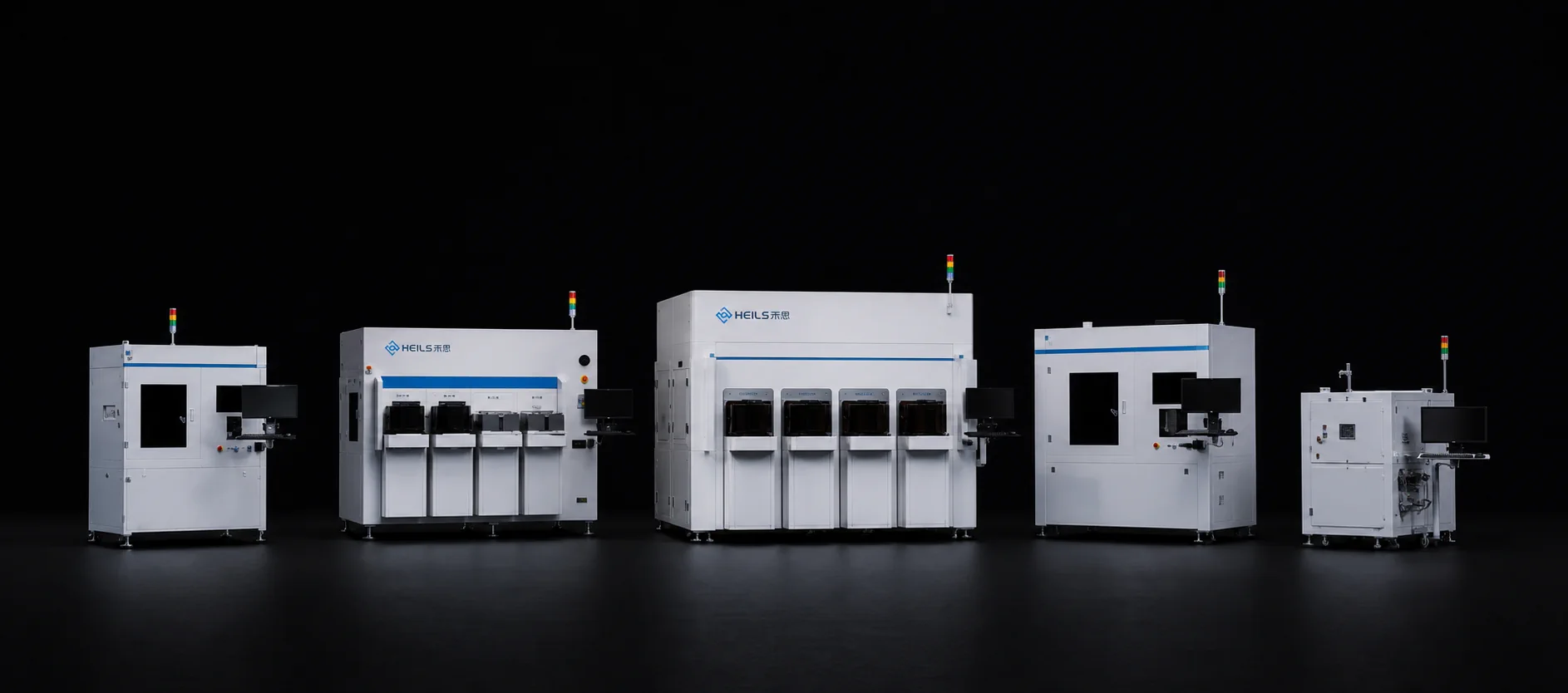
Glass Substrate Solution
Covers visual inspection, defect recognition, positioning review, and data traceability for glass substrate processes.
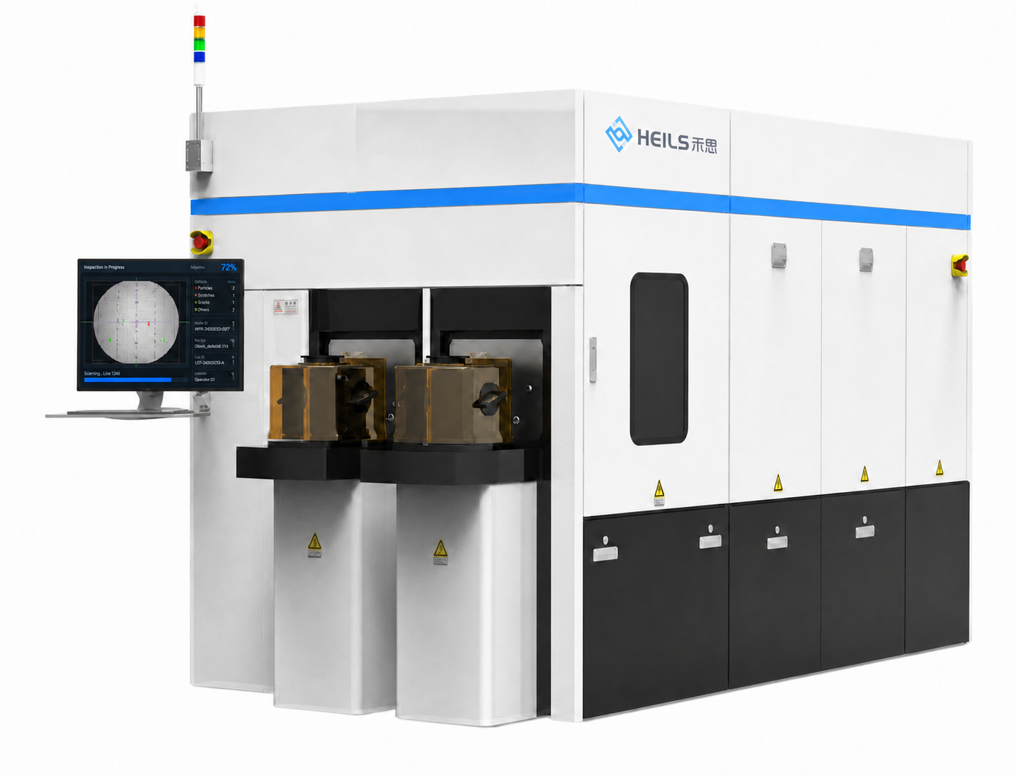
ME Series
M7000-T515PL Post-TGV Laser-Induced AOI Inspection System
The Post-TGV Laser-Induced AOI Inspection System M7000-T515PL delivers nanoscale precision inspection and closed-loop feedback control for laser-induced processes, ensuring the morphology, positional accuracy, and consistency of modified areas, effectively preventing via failures and abnormal metal filling. The system automatically synchronizes missing spot coordinates to the laser induction equipment, triggering precise supplementary processing to enhance yield and efficiency.
Product Advantages
Nanoscale Precision Inspection:Utilizes high-resolution imaging technology to accurately inspect the position, morphology, and array integrity of induced spots, supporting BF/DF imaging to meet stringent process requirements.
Closed-Loop Supplementary Control:Synchronizes missing or defective spot coordinates to the laser induction equipment in real time, automatically triggering supplementary processing commands for precise secondary processing, ensuring every via is complete.
Double-Side Full Inspection & Integrated Mapping:Performs full inspection on both the front and back sides of glass substrates, automatically integrates mapping, and unifies output results, covering defects such as presence/absence of modified areas, surface contamination, cracks, and burrs.
Broad Compatibility Design:Supports panel-level 510mm×515mm and wafer-level 6″, 8″, 12″ sizes, with thickness from 0.2 to 1.5mm, flexibly accommodating various incoming specifications.
Failure Prediction & Process Feedback:Identifies induced spots that may cause non-conductive etch holes in advance, providing data support for laser process parameter optimization and reducing downstream losses.
Product Functions
Product Specifications
- Compatible Substrate Size:
- Panel-level 510mm×515mm; Wafer-level 6″, 8″, 12″Supports multiple sizes simultaneously
- Incoming Thickness:
- 0.2-1.5mm
- Inspection Items:
- Presence/absence of modified area, surface contamination, cracks, burrsExtendable
- Inspection Range:
- Full inspection of front and back sides, automatic integrated mapping
- Throughput:
- 9 UPHSpeed can be increased based on actual inspection conditions
- Imaging Technology:
- BF/DF compatibleBright field/Dark field optional
Applications
Post-Laser-Induced Inspection of Glass Substrates:Used for rapid full inspection after laser-induced modification in TGV processes, ensuring induced spot quality and preventing subsequent etching and filling defects.
Wafer-Level Packaging AOI:Applicable for post-induced inspection of 6″, 8″, 12″ wafer-level glass substrates, combined with supplementary processing to improve packaging yield.
Advanced Semiconductor Packaging Lines:Integrated into glass substrate packaging lines to create a closed loop of inspection-feedback-supplementary processing, optimizing production flow and reducing process risk.
Display Panel & Microelectronic Substrate Manufacturing:Can be used for inspection of other glass or transparent substrates requiring high-precision laser modification, with expanded applications in panel-level packaging and more.