
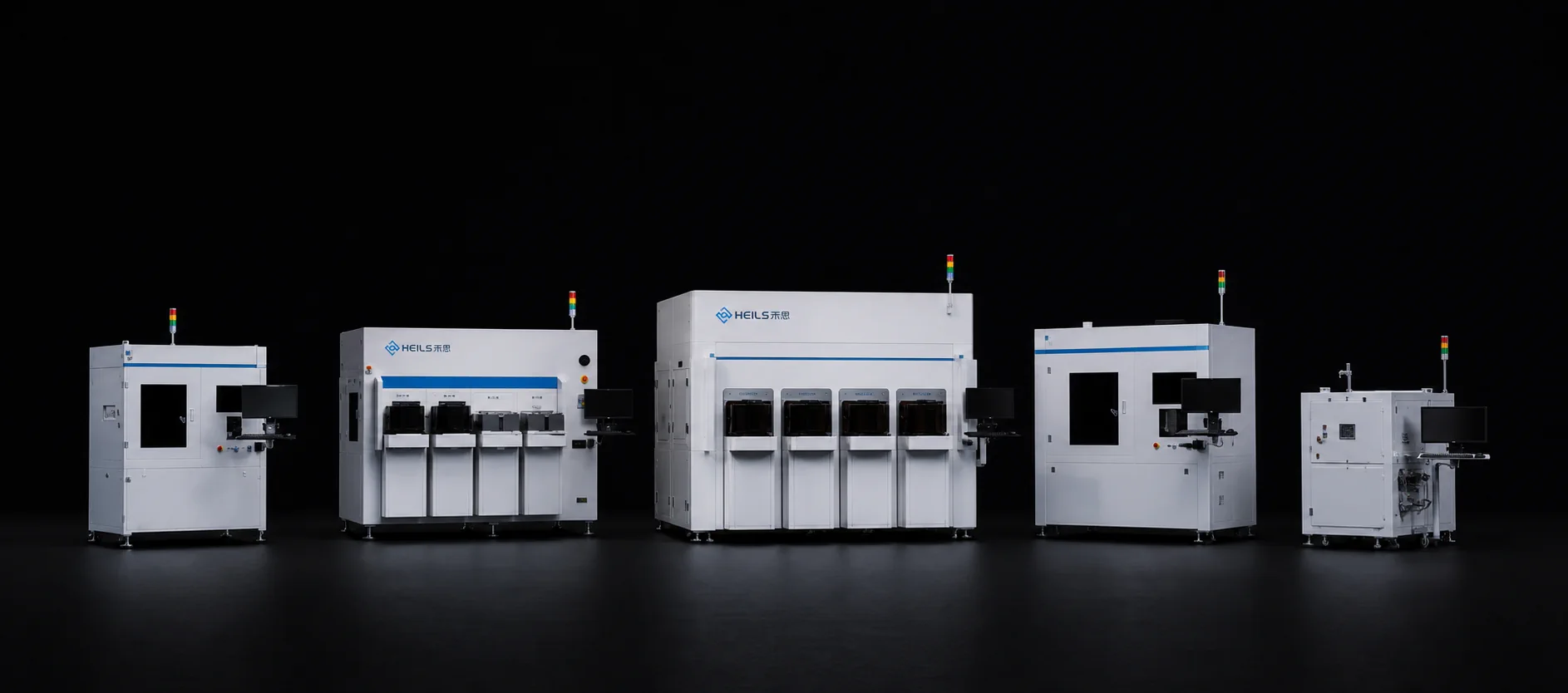
Advanced Ceramic Components
Focused on semiconductor ceramic devices, the solution covers full-site testing, inspection, sorting, and repair to improve chip reliability.
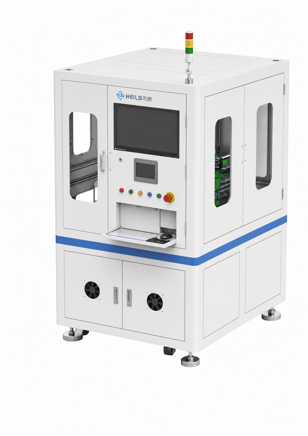
AMB, DBC, DPC Inspection Product Line
DBC001 Warpage/Thickness Inspection Equipment
This warpage/thickness inspection equipment is specifically designed for advanced ceramic substrates such as DBC and AMB. It utilizes a high-precision fitting stage and multi-point measurement comparison to achieve fast and accurate warpage and thickness inspection. The equipment offers ultra-high measurement accuracy and an extremely low misjudgment rate, effectively enhancing production line quality control.
Product Advantages
High-Precision Measurement:Employs high-resolution profile acquisition technology with 3200 points per profile, 12μm resolution on the XY axes, and 3.6μm accuracy on the Z axis, ensuring accurate capture of subtle deformations and thickness variations.
Low Misjudgment Rate:Overkill rate as low as 0.01% and miss rate as low as 0.001%, significantly reducing false positives and missed detections, improving yield and efficiency.
High-Efficiency Inspection:Inspection time of only 10 seconds per piece (for products sized 30-100mm), meeting production line takt time and improving inspection efficiency.
Wide Applicability:Compatible with various types of DBC and AMB substrates, supporting multiple sizes and shapes to flexibly adapt to diverse production needs.
Intelligent Data Analysis:Automatically compares the fitting stage and measurement points, rapidly outputting height difference data, and supporting integration into automated production lines.
Product Functions
Product Specifications
- Inspection Object:
- Warpage/Thickness
- Profiles per Point:
- 3200
- XY Axis Resolution:
- 12μm
- Z Axis Accuracy:
- 3.6μm
- Overkill Rate:
- 0.01%Varies by defect type
- Miss Rate:
- 0.001%Varies by defect type
- Inspection Efficiency:
- 10 sec/pieceFor products sized 30-100mm
Applications
DBC Substrate Inspection:Used for warpage and thickness measurement of direct bonded copper ceramic substrates to ensure packaging reliability.
AMB Substrate Inspection:Applied to quality control of active metal brazed ceramic substrates, ensuring the performance of power electronics modules.
Advanced Ceramic Components:Suitable for online inspection of ceramic substrates such as aluminum nitride and alumina, supporting semiconductor packaging and IGBT module manufacturing.
Production Line Quality Monitoring:Integrated into automated production lines to monitor warpage and thickness indicators in real time, improving overall yield.