
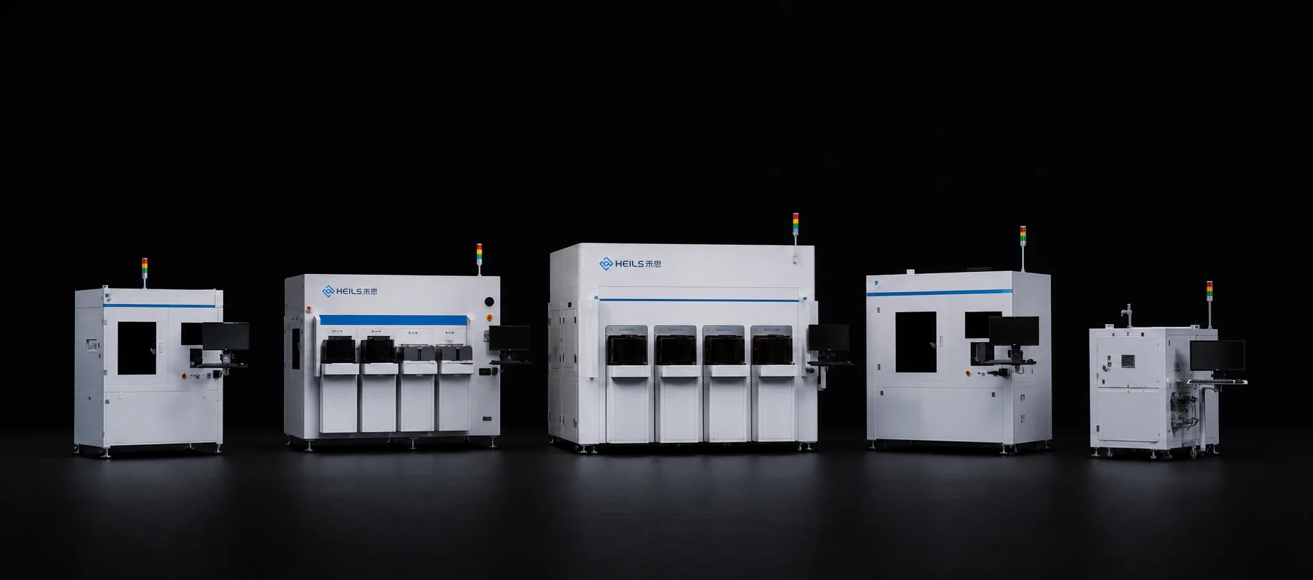
Advanced Ceramic Components
Focused on semiconductor ceramic devices, the solution covers full-site testing, inspection, sorting, and repair to improve chip reliability.
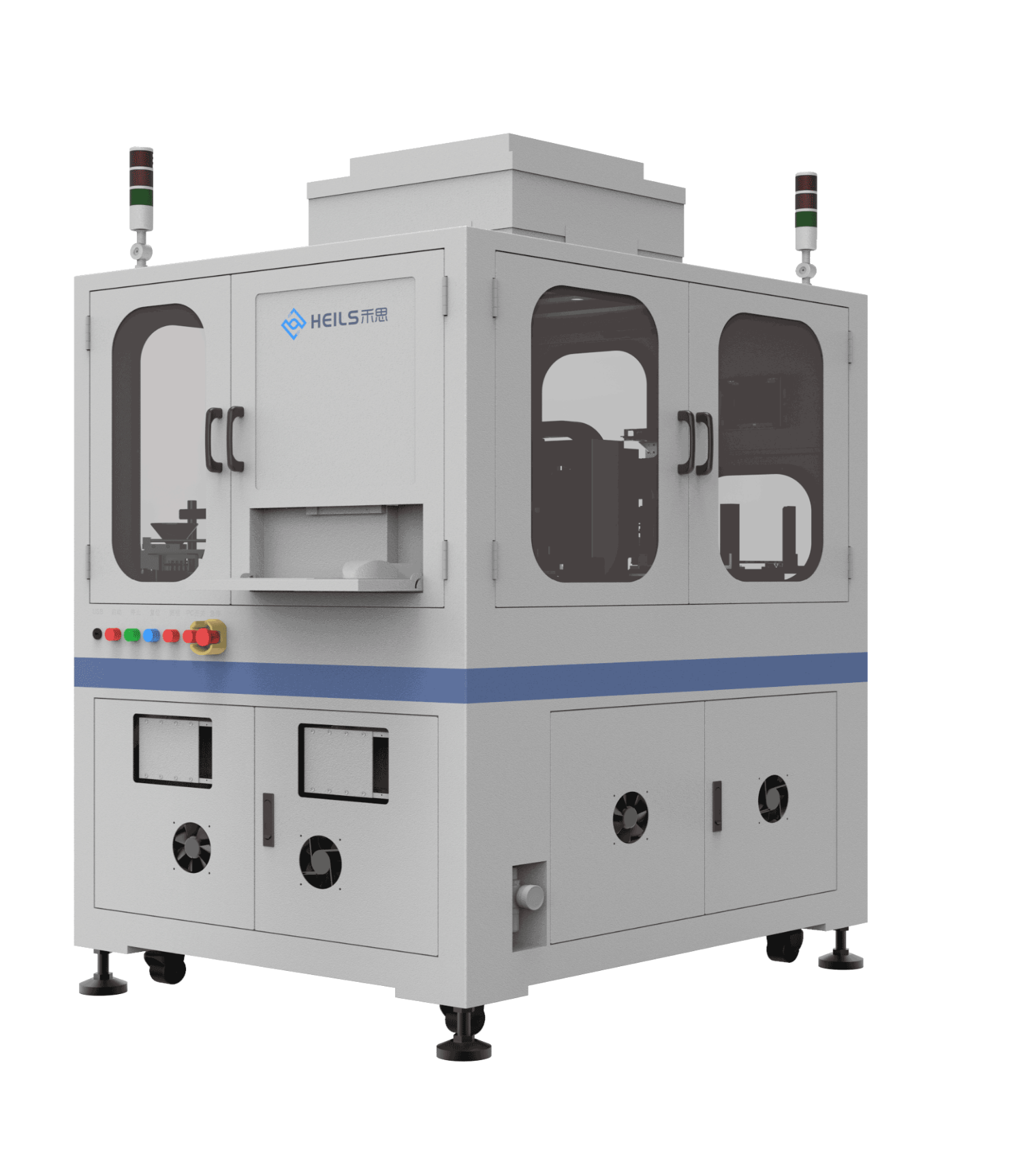
Thin-Film Circuit Inspection System
FP003 Thin-Film Circuit Inspection Equipment
This equipment is purpose-built for the visual defect inspection of high-precision thin-film circuits on ceramic substrates. Featuring a high-resolution imaging system, it achieves pixel accuracy of 1 μm and repeatability of ±1 μm, automatically identifying defects such as circuit opens, missing traces, excess metal, offset, and contamination while simultaneously performing dimensional measurement, delivering efficient and reliable quality assurance for advanced ceramic components.
Product Advantages
High-Precision Inspection:Pixel accuracy up to 1 μm and repeatability of ±1 μm enable precise identification of micron-level defects, meeting the requirements of high-end ceramic circuit manufacturing, with selectable accuracy grades to suit different product needs.
Comprehensive Defect Coverage:Detects more than ten defect types—including circuit opens, missing traces, excess metal, offset, contamination, foreign matter, burrs, color variation, jagged edges, and chipping—while completing dimensional measurement to ensure product quality.
Superior Inspection Performance:With an over-kill rate of only 0.1% and an escape rate as low as 0.01%, it greatly reduces false judgments and escapes while ensuring inspection quality, effectively lowering production costs.
High Inspection Efficiency:For a 2-inch product, inspection takes only 5 seconds per piece, suitable for high-volume production takt times and improving overall line efficiency.
Smart Data Export:Automatically generates new DXF files from recognized images, facilitating data traceability, process optimization, and subsequent analysis, enabling seamless integration between inspection and manufacturing.
Product Functions
Product Specifications
- Inspection Target:
- Thin-film circuitsHigh-precision circuits on ceramic substrates
- Max Accuracy:
- Pixel accuracy 1 μm, repeatability ±1 μmSelectable accuracy grades
- Standard Accuracy:
- Pixel accuracy 3 μm, repeatability ±3 μmThe data below is based on standard accuracy
- Inspection Content:
- Circuit opens, missing traces, excess metal, offset, contamination, foreign matter, burrs, color variation, jagged edges, chipping, etc.Generates and exports DXF from recognized images
- Over-Kill Rate:
- 0.1%
- Escape Rate:
- 0.01%
- Inspection Efficiency:
- 5s/pcsFor 2-inch products
Applications
Thin-Film Circuits on Ceramic Substrates:Suitable for visual defect inspection and dimensional measurement of high-precision thin-film circuits formed on ceramic substrates by sputtering and photolithography processes.
Advanced Ceramic Components:Used for circuit pattern inspection in advanced ceramic components to ensure product performance and reliability.
Semiconductor Package Substrate Inspection:In the semiconductor packaging field, it enables rapid inspection of fine circuits on ceramic package substrates, meeting high-reliability requirements.
Microelectronic Device Manufacturing:Applied to quality control of thin-film circuits in microelectronic device manufacturing, helping improve yield and production efficiency.