
Advanced Ceramic Components
Focused on semiconductor ceramic devices, the solution covers full-site testing, inspection, sorting, and repair to improve chip reliability.
HTCC / LTCC Finished Product Line
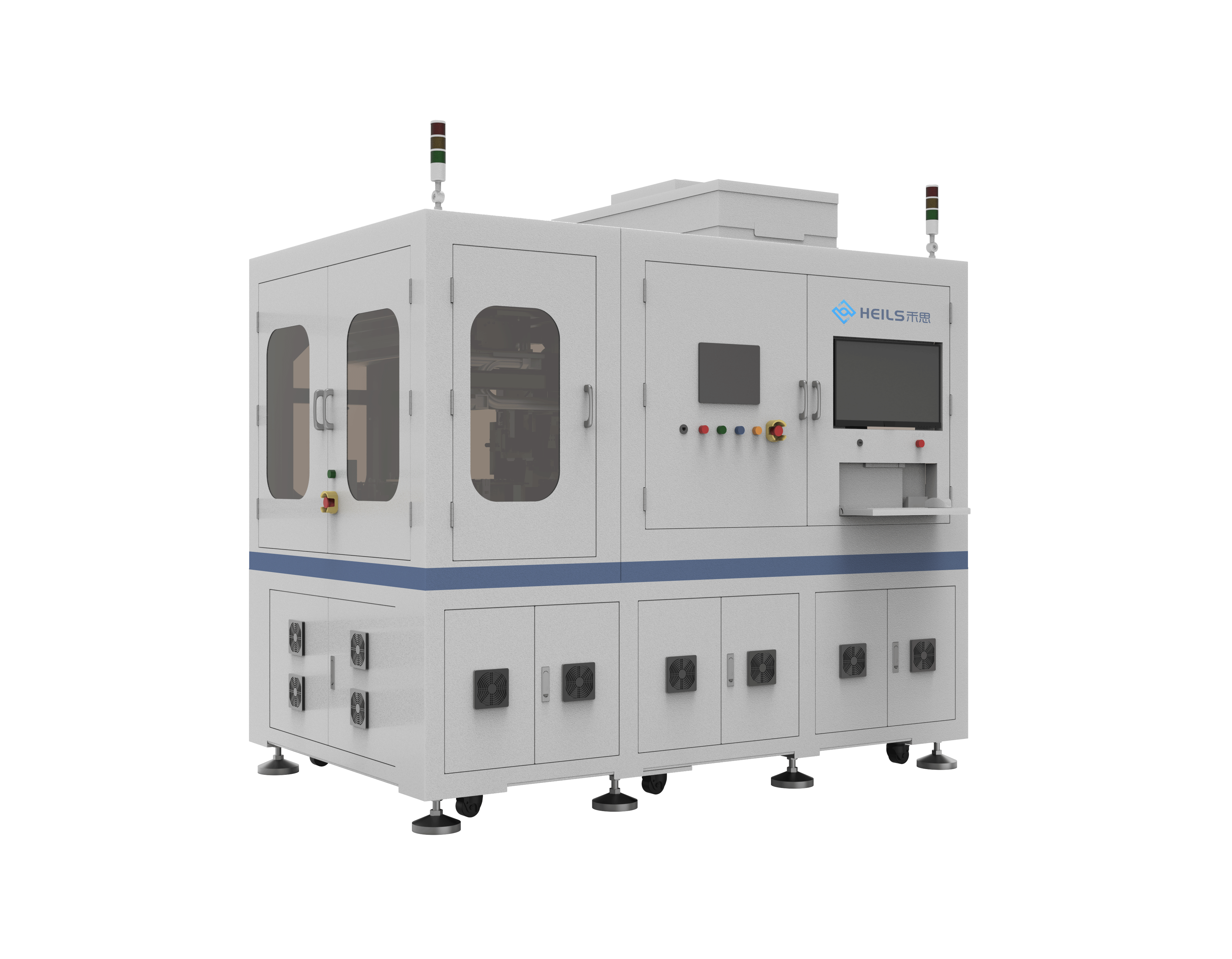
FP001 Appearance Inspection Equipment (Crystal Oscillator Finished Products)
The FP series appearance inspection equipment is specifically designed for advanced ceramic components such as finished crystal oscillators. It enables efficient and high-precision appearance inspection before dicing of the entire substrate, supporting gold-plated HTCC sintered ceramic products, crystal oscillator bases, ceramic substrates, etc. With a pixel accuracy of 2.1μm and detection accuracy of 10μm, the equipment accurately identifies defects such as seal ring misalignment, pattern defects, pits/bumps, ceramic black spots, etc. The overkill rate is only 0.1%, the miss rate is 0.01%, and the inspection time per piece is 0.02 seconds, contributing to finished product screening and process control.
Product Advantages
High-Precision Inspection:With a pixel accuracy of 2.1μm and detection accuracy of up to 10μm, it precisely captures subtle defects, ensuring high-quality finished product screening.
High-Efficiency Whole-Board Inspection:Inspection is performed on a whole-board basis, completing appearance checks before dicing, with an inspection time of only 0.02 seconds per piece, greatly improving efficiency and suitable for mass production.
Comprehensive Defect Coverage:Capable of detecting over ten types of defects including seal ring misalignment, pattern defects, pits/bumps, ceramic black spots, excessive solder, missing ceramic, foreign matter, scratches, and poor overlap, meeting quality control needs across multiple process steps.
Extremely Low False Rejection Rate:With an overkill rate of only 0.1% and a miss rate of only 0.01%, it reduces material waste from false detections while ensuring inspection quality, improving production yield.
Product Functions
Product Specifications
- Pixel Accuracy:
- 2.1μm
- Detection Accuracy:
- 10μm
- Inspection Time per Piece:
- 0.02s/pcs
- Overkill Rate:
- 0.1%
- Miss Rate:
- 0.01%
- Inspection Target:
- Gold-plated HTCC sintered ceramic products before dicing, crystal oscillator bases, ceramic substrates, SAW substrates, etc.Whole board finished products
Applications
Crystal Oscillator Finished Product Inspection:For crystal oscillator bases and finished products, inspects seal rings, patterns, and surface defects before dicing to ensure the quality and reliability of crystal oscillators.
Ceramic Substrate Inspection:Applicable to appearance inspection of ceramic substrates, identifying defects such as pits, bumps, and black spots to ensure substrate performance.
HTCC Product Inspection:Used for whole-board inspection of HTCC sintered ceramic products, promptly identifying process abnormalities and improving product yield.
SAW Substrate Inspection:Inspects printing, patterns, and surface defects of surface acoustic wave substrates, meeting the requirements of high-precision electronic components.