
Advanced Ceramic Components
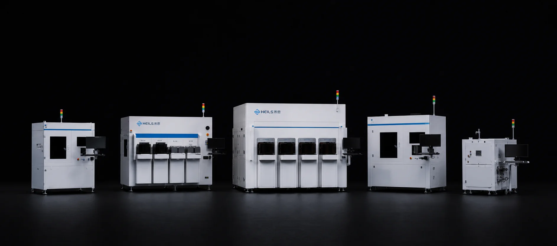
Focused on semiconductor ceramic devices, the solution covers full-site testing, inspection, sorting, and repair to improve chip reliability.
HTCC / LTCC Green Tape Product Line
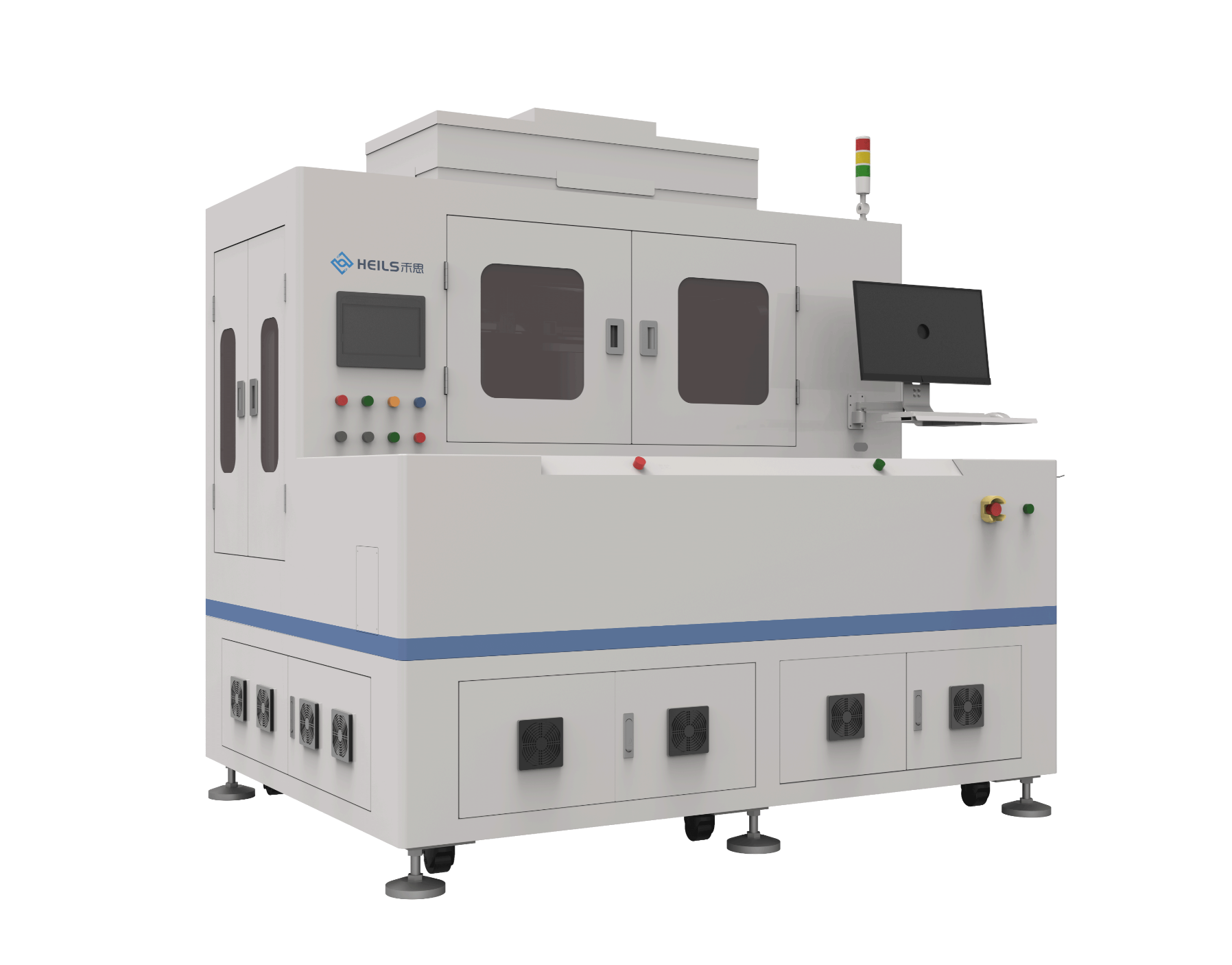
ME3555 Large-Size Green Sheet Appearance Inspection Equipment
The ME Large-Size Green Sheet Appearance Inspection Equipment is specifically designed for green sheets used in electrostatic chucks and probe cards. It covers full inspection for through-holes, via filling, and printing processes, supporting large-size sheets from 350 to 550 mm. With sub-micron precision, it enables efficient defect detection, aiding quality control in advanced ceramic component manufacturing.
Product Advantages
High-Precision Inspection:Equipped with a super-depth-of-field camera, it achieves imaging precision up to 0.4 μm, pixel accuracy of 2.6 μm at standard precision, and repeatability of ±1 μm, reliably capturing fine defects to meet stringent process requirements.
Large-Size Compatibility:Supports inspection of large ceramic sheets from 350 to 550 mm, accommodating large green sheets for electrostatic chucks and probe cards. Manual loading/unloading design flexibly adapts to production workflows.
Comprehensive Process Coverage:Provides comprehensive inspection items for various processes such as through-holes, via filling, printing, and bars, including foreign matter in holes, roundness, via dimples, via height, pattern shift, line width anomalies, and more, enabling one-stop full inspection.
Smart Zone Inspection:Supports DXF file import and customizable zone-based inspection strategies to optimize inspection efficiency, particularly suitable for complex pattern areas on large-size sheets.
Extremely Low False Positives and Missed Defects:Overkill rate is controlled within 0.1%, and missed detection rate is as low as 0.03%, ensuring accurate defect capture and minimizing the impact of misjudgment on production efficiency.
With Super Depth-of-Field Technology:Combined with super depth-of-field technology, it quickly identifies specific via height values, ensuring accurate defect capture and reducing the impact of uneven via height on the production process.
Product Functions
Product Specifications
- Maximum Inspection Size:
- 550mmSupports sheets from 350 to 550 mm
- Pixel Accuracy:
- 2.6μmStandard precision; up to 1 μm optional
- Repeatability:
- ±1μmPrecision levels supported
- Super Depth-of-Field Camera Imaging Precision:
- 0.4μm
- Inspection Speed:
- 3 min/pieceFor a 500 mm sheet as an example
- Overkill Rate / Missed Detection Rate:
- 0.1% / 0.03%Both are typical values
Applications
Green Sheet Inspection for Electrostatic Chucks:Applies to full appearance inspection after through-hole, via filling, and printing processes in electrostatic chuck manufacturing, ensuring hole position accuracy and via filling quality.
Green Sheet Inspection for Probe Cards:Performs high-precision inspection of micro through-holes, via filling, and printed patterns on probe card sheets, ensuring signal transmission reliability.
Large Ceramic Substrate Printing Inspection:Used for appearance defect inspection of printed circuits, electrode patterns, etc., such as breaks, continuity, and misalignment, suitable for large substrates from 350 to 550 mm.