
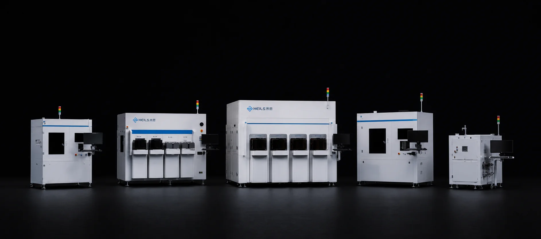
Advanced Ceramic Components
Focused on semiconductor ceramic devices, the solution covers full-site testing, inspection, sorting, and repair to improve chip reliability.
HTCC / LTCC Green Tape Product Line
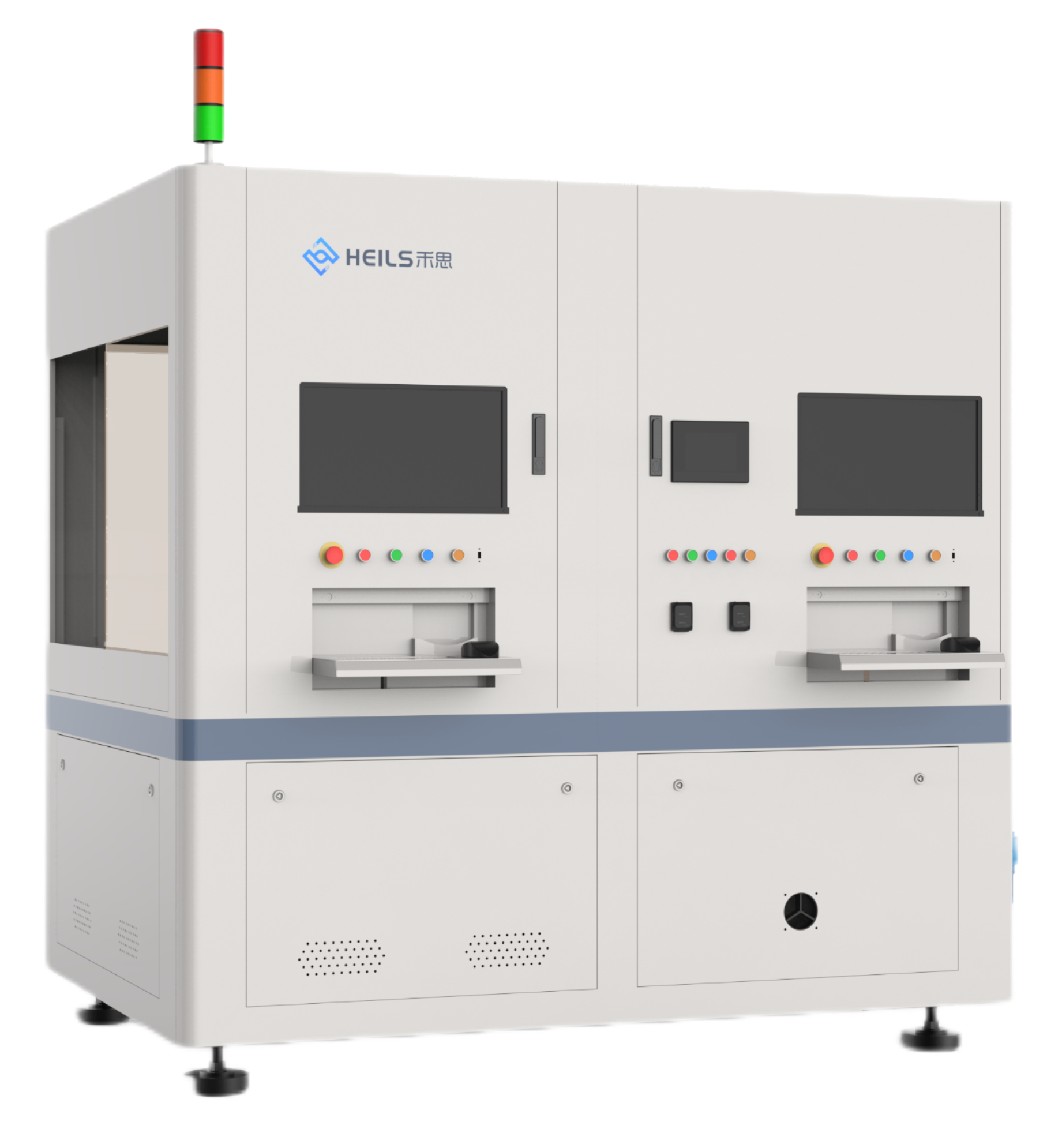
GR3500 Appearance Inspection Equipment - High-Precision Printed Patterns
The ME inspection machine series appearance inspection equipment is specifically designed for high-precision inspection of printed patterns on advanced ceramic components. It is suitable for appearance inspection of various surface patterns and circuits such as screen printing, photolithographic circuits, and etched circuits at different process stages of green/ fired ceramics, covering products like LTCC/HTCC printed sheets, resistors, thin-film circuits, and thick-film circuits. With high precision, high efficiency, and low false rejection rate, it ensures production quality.
Product Advantages
Ultra-High Precision Inspection:Maximum pixel accuracy of 1 μm and repeat accuracy of ±1 μm; common accuracy is pixel 3 μm and repeat accuracy ±3 μm. Supports accuracy grading to meet stringent requirements of different process stages.
Comprehensive Defect Detection:Detects a wide range of defects including open circuits, shorts, whiskers, missing parts, overflow, ink bleeding, pinholes, bumps, dents, pattern misalignment, abnormal line width, abnormal spacing, surface foreign matter, missing patterns, extra patterns, and via filling defects.
Extremely Low False Rejection Rate:With an over-kill rate of only 0.01% and a miss rate of only 0.001%, it ensures high reliability and reduces cost losses caused by misjudgments.
High-Efficiency Inspection Capability:Inspection time for 200 mm products is only 6 seconds per piece, meeting the high-speed takt requirements of production lines.
Smart Marking and Traceability:After identifying NG, laser micro-machining or laser/inkjet marking can be performed, and unified marking after stacking NG data is supported for easy traceability and downstream processing.
Product Functions
Product Specifications
- Inspection Object:
- Screen printing / Photolithographic circuits / Etched circuitsApplicable to various process stages
- Maximum Accuracy:
- Pixel 1 μm, repeat ±1 μmSupports accuracy grading
- Common Accuracy:
- Pixel 3 μm, repeat ±3 μm
- Inspection Efficiency:
- 6 s/pieceFor 200 mm products
- Over-kill Rate:
- 0.01%
- Miss Rate:
- 0.001%
Applications
LTCC/HTCC Printed Sheets:Inspects printed patterns on green/fired ceramic sheets to ensure circuit integrity, suitable for multi-layer ceramic substrate manufacturing.
Thin-Film and Thick-Film Circuits:Applied to appearance inspection of thin-film and thick-film circuits, ensuring pattern accuracy and surface quality.
Resistors and Conductor Circuits:Inspects the printing quality of resistors and conductor circuits, controlling key parameters such as line width and spacing.