
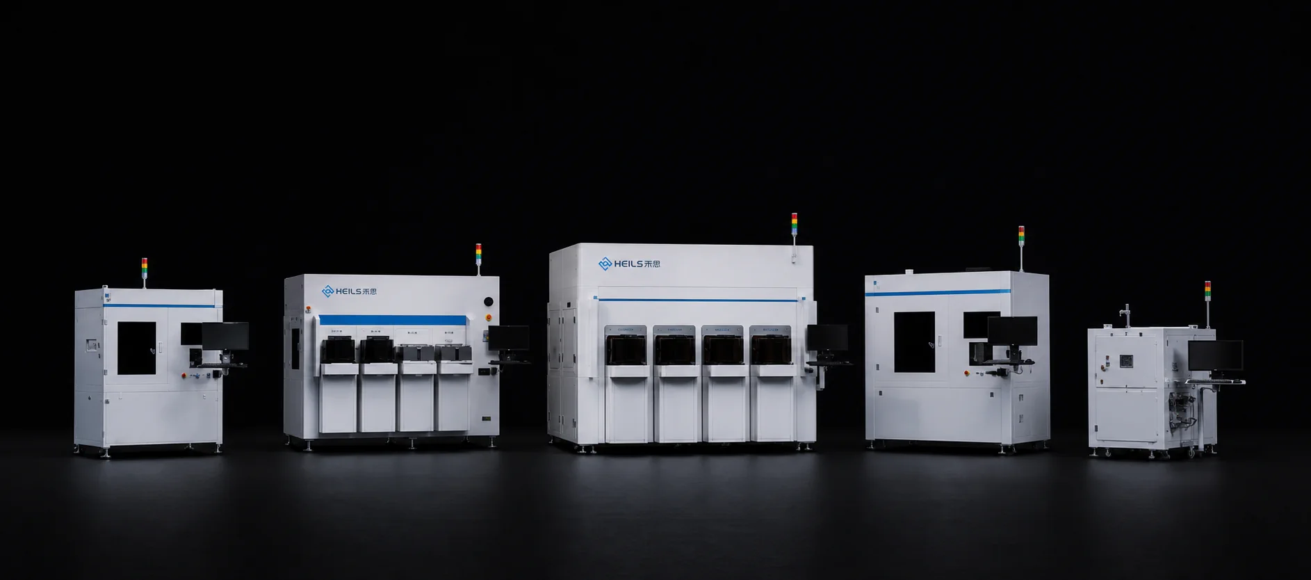
Advanced Ceramic Components
Focused on semiconductor ceramic devices, the solution covers full-site testing, inspection, sorting, and repair to improve chip reliability.
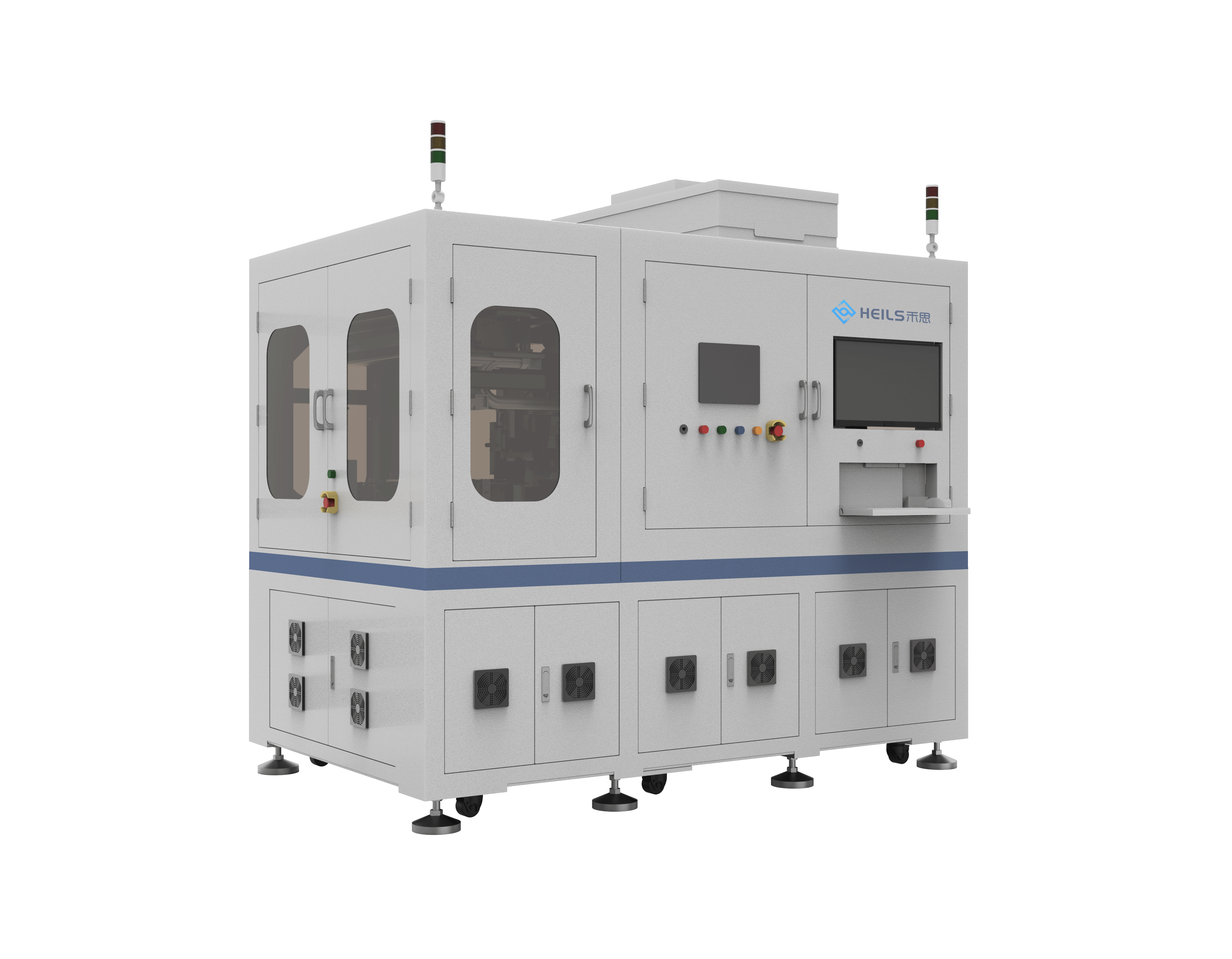
HTCC / LTCC Finished Product Line
FP002 Appearance Inspection Equipment (Finished Ceramic Packages)
The FP series appearance inspection equipment is specifically designed for finished ceramic packages. With a 360° rotating axis, it enables comprehensive multi-angle inspection, accurately identifying minute defects such as scratches, cracks, and chips. The system delivers high precision, high efficiency, and an extremely low false rejection rate, making it an ideal choice for quality assurance of advanced ceramic components.
Product Advantages
Full-Angle Coverage Inspection:Equipped with a 360° rotating axis that supports rotation at any angle, enabling comprehensive multi-angle inspection of various types of ceramic packages, including lead frame, leaded, and optical window types, with no blind spots.
High-Precision Imaging System:Utilizes a high-resolution camera with a pixel accuracy of 2.1μm and detection accuracy of 10μm, effectively identifying sub-millimeter defects and ensuring no tiny flaws are missed.
Comprehensive Defect Detection Capability:Covers over 20 defect types including scratches, cracks, dents and bumps, chips, bubbles, gold layer peeling, contamination, overflow, foreign matter, flatness, color deviation, plating voids, burrs, missing parts, delamination, holes, solder buildup, misalignment, and internal cavity defects, meeting diverse inspection needs.
Extremely Low False Rejection and Missed Detection:Utilizing advanced algorithm optimization, the overkill rate is only 0.1% and the missed detection rate is as low as 0.01%, ensuring reliability while significantly reducing manual reinspection costs.
High-Speed Inspection Takt Time:The inspection cycle per part is only 5 seconds (taking the inspection of 11 surfaces of an optical communication package as an example), balancing high precision and high throughput to meet production line takt time requirements.
Product Functions
Product Specifications
- Inspection Object:
- Finished ceramic packages (lead frame, leaded, optical window, etc.)
- Pixel Accuracy:
- 2.1μm
- Detection Accuracy:
- 10μm
- Overkill Rate:
- 0.1%False rejection rate
- Missed Detection Rate:
- 0.01%
- Inspection Efficiency:
- 5s/pcsFor optical communication packages, inspecting 11 surfaces
Applications
Optical Communication Devices:Suitable for surface defect inspection of optical communication components such as optical communication packages, ensuring high reliability and optical performance.
Semiconductor Packaging:Used for finished inspection of ceramic packages for semiconductor packaging, ensuring packaging quality and electrical performance.
Electronic Components:Inspects housing defects of various ceramic electronic components, improving product consistency and service life.
Aerospace and Military:Meets high-reliability requirements for inspecting ceramic packaging housings used in aerospace, military, and other fields, ensuring stability under extreme environments.