

Advanced Ceramic Components
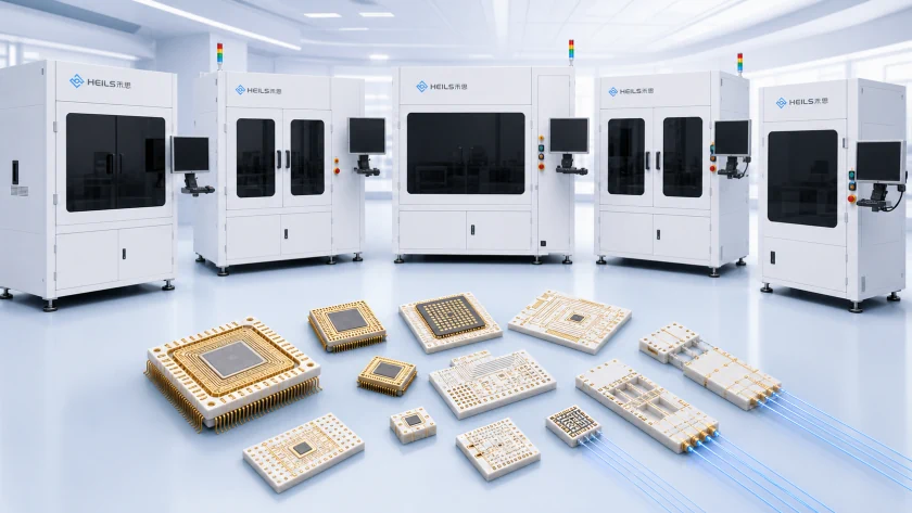
Focused on semiconductor ceramic devices, the solution covers full-site testing, inspection, sorting, and repair to improve chip reliability.
Splitting & Sorting
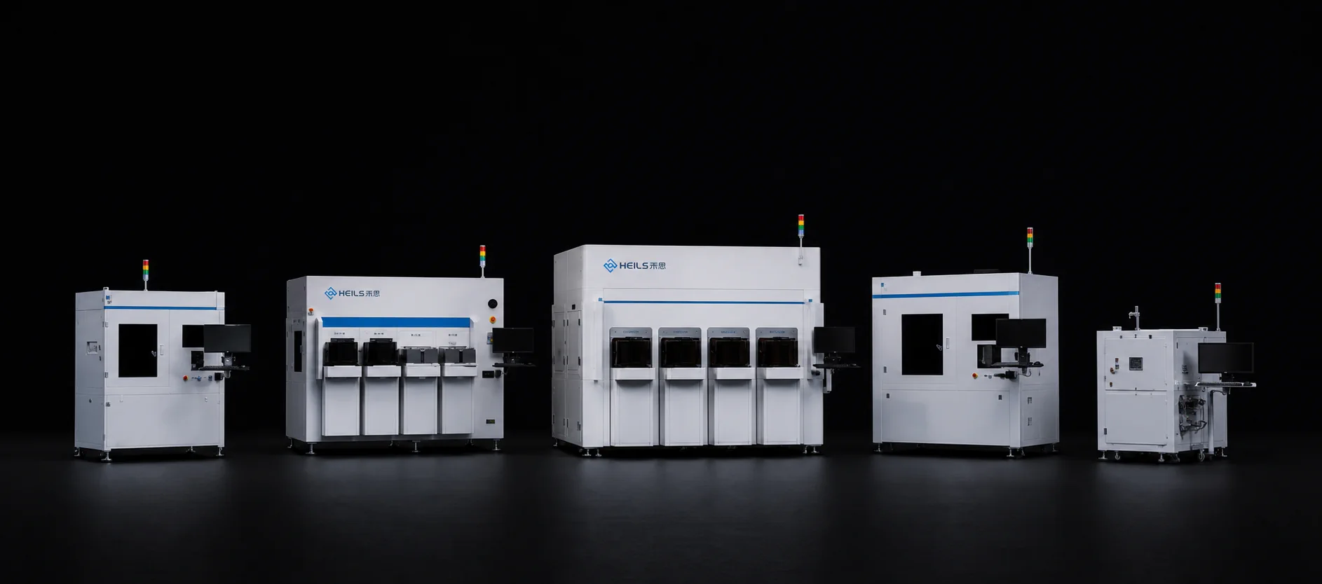
测试型号 Test Equipment
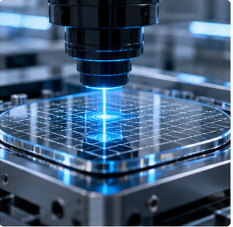
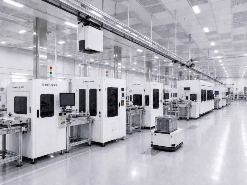
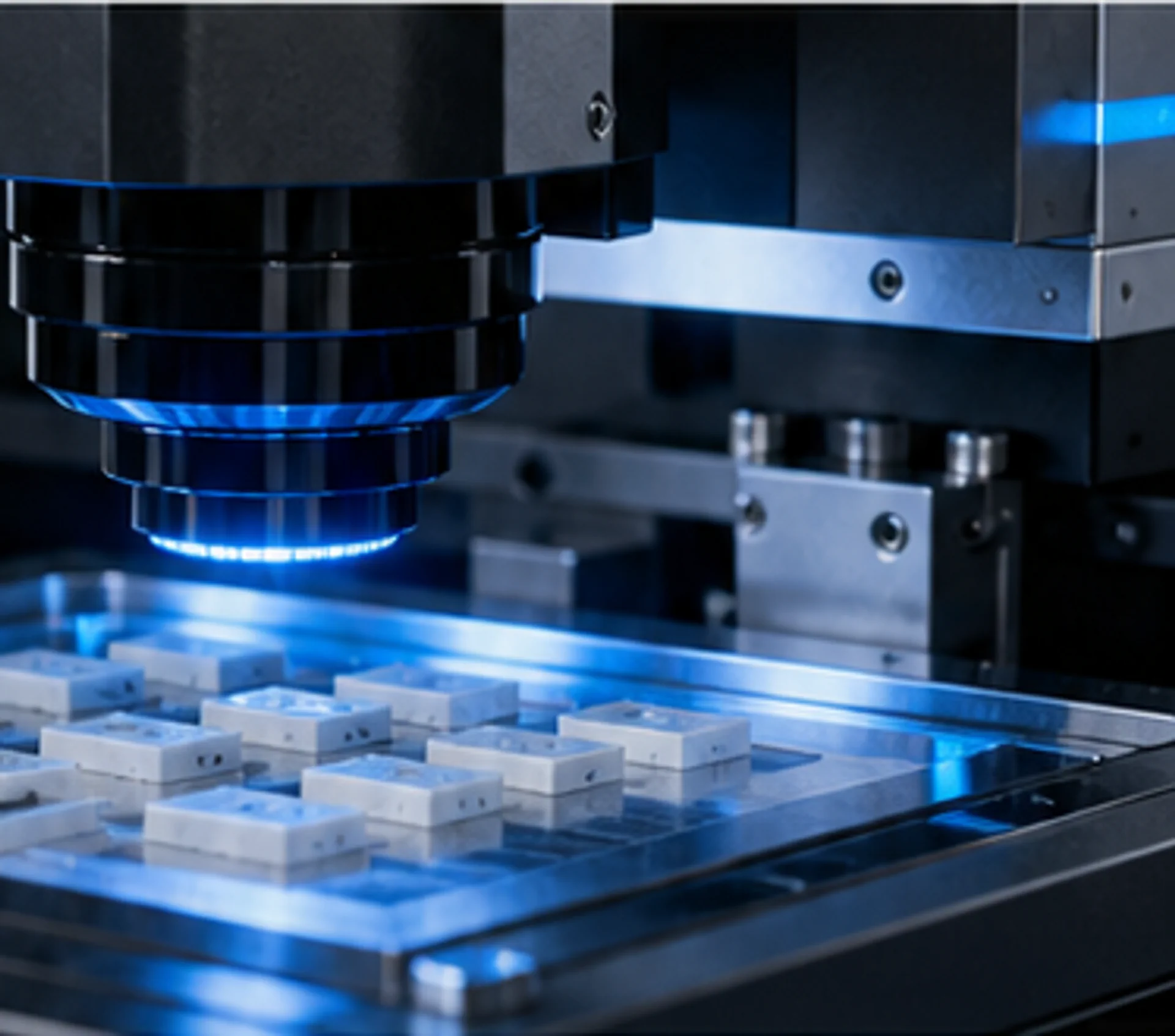
The high-precision laser processing test equipment is specifically designed for advanced ceramic components, supporting multi-station cooperative laser drilling to significantly improve processing efficiency and consistency. With stable and reliable performance, it meets the high standards of B2B industrial inspection equipment.
Product Advantages
Multi-Station Cooperative Processing:Supports simultaneous operation of multiple stations, achieving efficient laser drilling through coordinated control, greatly reducing production cycle time.
High-Precision Positioning:Employs a precision motion stage and vision alignment system to ensure hole position accuracy at the micron level, meeting stringent tolerance requirements for ceramic components.
Stable Laser Source:Equipped with an industrial-grade laser, providing stable output energy and adjustable pulse width, suitable for ceramic processing of various thicknesses and materials.
Intelligent Monitoring and Feedback:Real-time monitoring of processing parameters, automatic deviation compensation to ensure batch consistency, and supports data traceability.
Product Functions
Product Specifications
- Number of Stations:
- 2-4Optional based on configuration
- Positioning Accuracy:
- ±5 μm
- Laser Wavelength:
- 355 nmOther wavelengths customizable
- Max Processing Size:
- 300 × 300 mm
- Processing Efficiency:
- >100 holes/minDepends on hole diameter and material
Applications
Ceramic Substrate Drilling:Applicable for precision through-hole and blind-hole processing of ceramic substrates such as alumina and aluminum nitride, used in electronic packaging and heat dissipation structures.
Micro-Hole Processing for Ceramic Structural Components:Meets the micro-hole array processing needs of complex structures like ceramic nozzles and insulators, with controllable hole diameter range of 50-500 μm.