
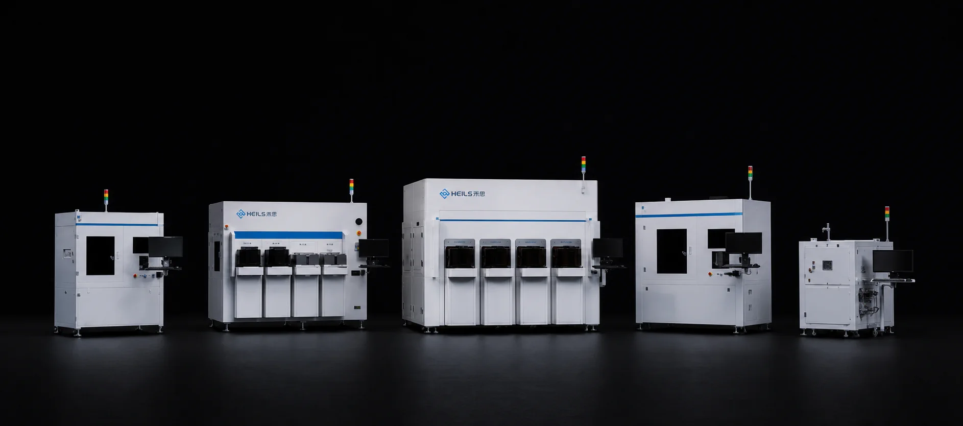
Advanced Ceramic Components
Focused on semiconductor ceramic devices, the solution covers full-site testing, inspection, sorting, and repair to improve chip reliability.
HTCC / LTCC Green Tape Product Line
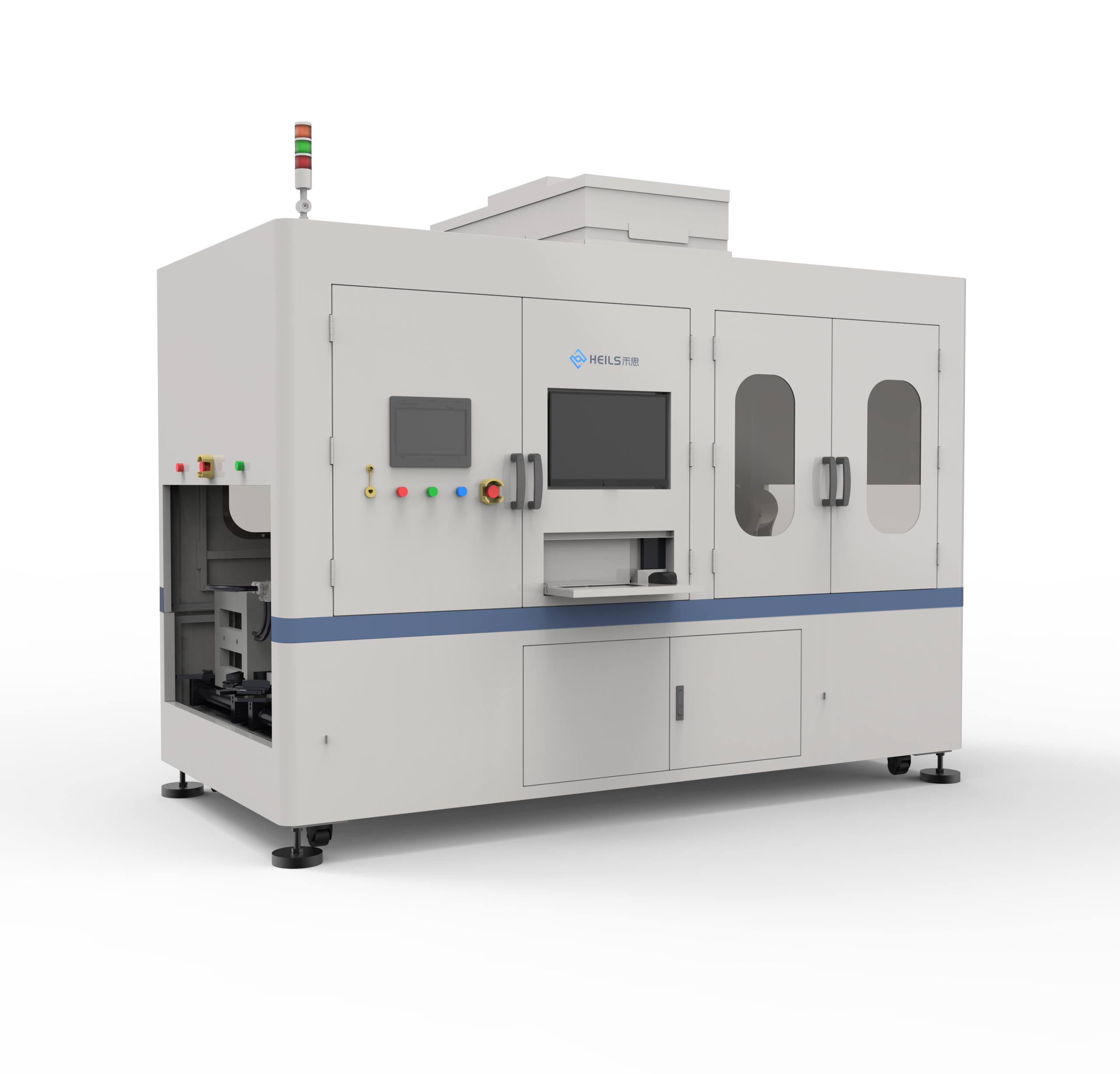
ME2000 Ceramic Through-Hole Inspection Equipment
The ME2000 ceramic through-hole inspection system is designed for high-precision inspection of ceramic through-holes, supporting inspection of up to 10 million holes with a maximum accuracy of 1 micron. The equipment offers excellent operability, supports DXF and Gerber file import, and is widely used in ceramic substrates, LTCC, HTCC, and other fields.
Product Advantages
Ultra-High Through-Hole Inspection Capability:Supports inspection of up to 10 million through-holes, meeting the mass production needs of large-scale ceramic substrates.
Micron-Level Inspection Accuracy:Maximum inspection accuracy reaches 1 micron, ensuring the dimensional and positional accuracy of tiny through-holes.
Convenient File Import:Supports direct import of DXF and Gerber files, simplifying the programming process and improving efficiency.
Superior Operability:User-friendly interface and automated processes lower the operation threshold and reduce human error.
Product Functions
Product Specifications
- Maximum Inspection Count:
- 10,000,000 holes
- Inspection Accuracy (Max):
- 1 μm
- Supported File Formats:
- DXF, Gerber
- Applicable Products:
- Ceramic substrates, LTCC, HTCC, etc.
Applications
Ceramic Substrate Through-Hole Inspection:Used for dimensional and defect inspection of high-density through-holes in ceramic packaging substrates.
LTCC/HTCC Process Inspection:Applicable to through-hole quality inspection in low-temperature co-fired ceramic and high-temperature co-fired ceramic products.
Microelectronics Packaging Inspection:Meets the high-precision inspection requirements for ceramic substrate through-holes in advanced packaging.
MEMS Device Inspection:Used for automated inspection of micron-level through-holes in ceramic substrates for MEMS.