

Advanced Ceramic Components
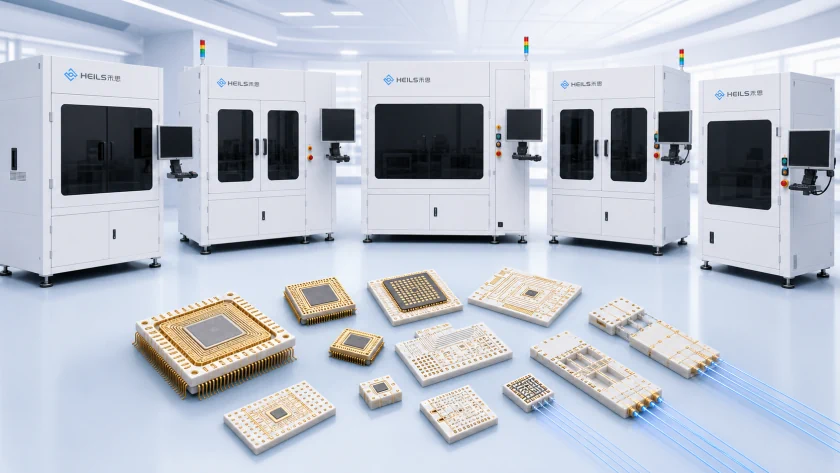
Focused on semiconductor ceramic devices, the solution covers full-site testing, inspection, sorting, and repair to improve chip reliability.
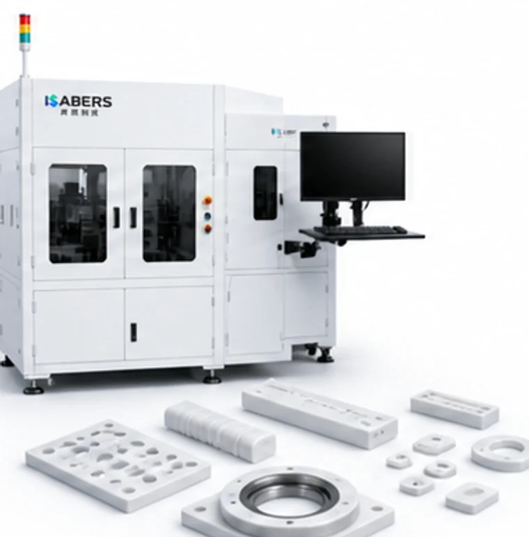
Vision Inspection
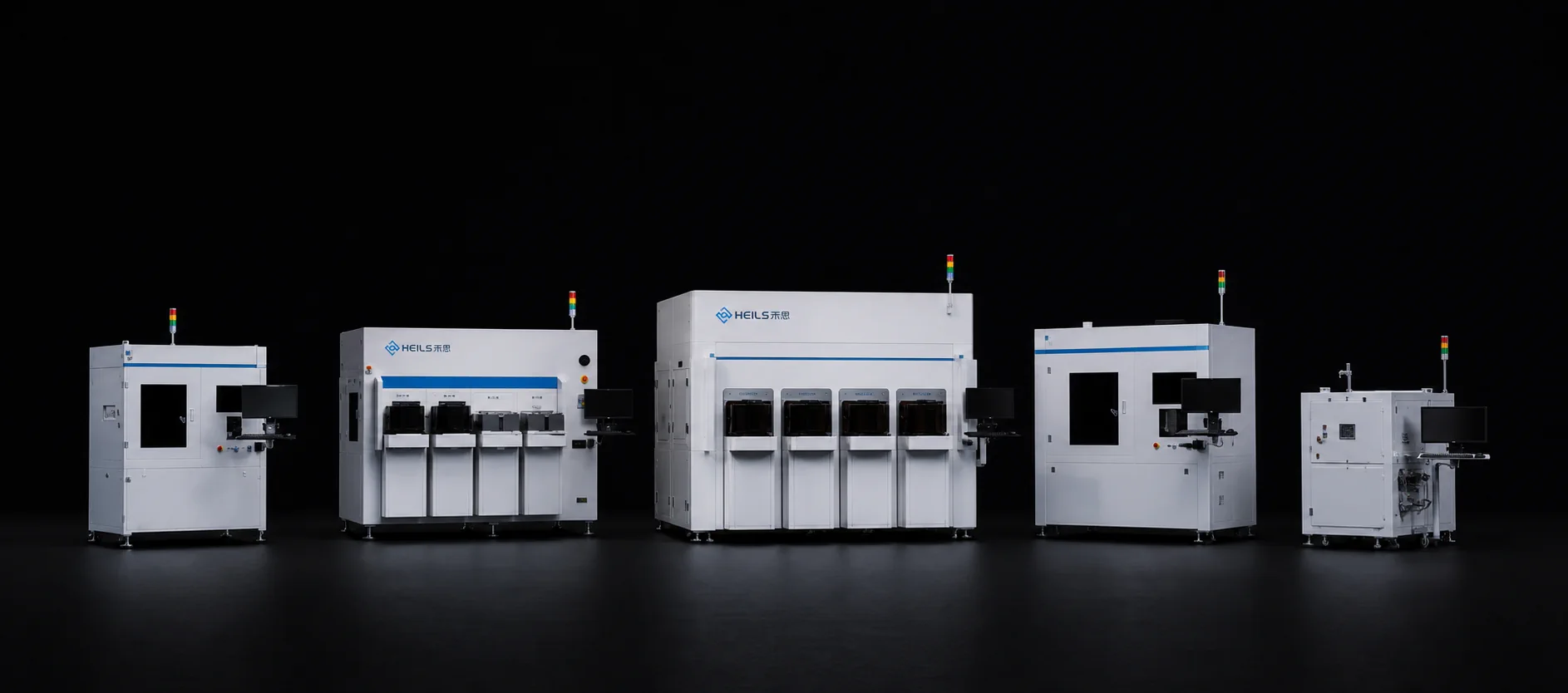
TKF500 Inspection Equipment
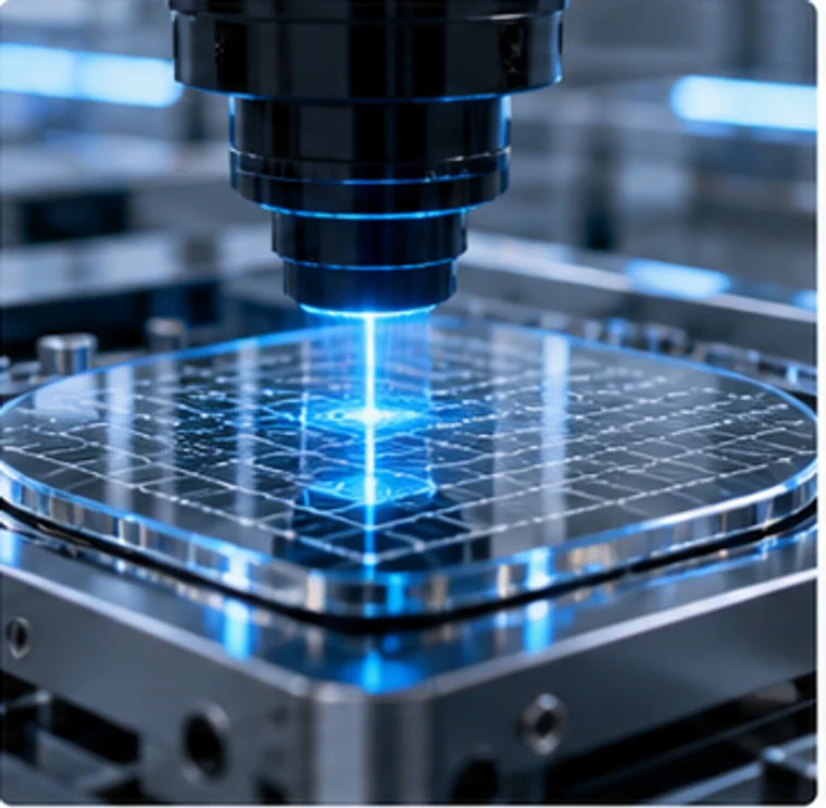
This equipment is dedicated to appearance defect detection of semiconductor ceramic components, accurately identifying surface cracks, bumps, contamination, and metal foreign objects, enabling efficient full inspection. It uses high-resolution industrial cameras and intelligent algorithms to ensure detection stability and accuracy, helping to improve yield rate.
Product Advantages
High-Precision Defect Detection:Equipped with high-resolution line scan cameras and multi-angle lighting, it accurately detects tiny defects such as cracks, bumps, contamination, and metal foreign objects, with a minimum detectable defect size of 0.02 mm.
High Throughput:Inspection speed up to 2000 UPH, meeting high-volume production line cycle time requirements, ensuring full inspection without missing defects.
Customizable Inspection Solutions:Inspection algorithms and optical configurations can be flexibly adjusted for different product forms such as ceramic substrates and packages, adapting to diverse needs.
Stable and Reliable Operation:Industrial-grade hardware architecture and anti-vibration design ensure operation in 24/7 continuous production environments, with easy maintenance and reduced downtime risk.
Product Functions
Product Specifications
- Inspection Speed:
- 2000 UPHStandard mode, adjustable based on product size and defect complexity
- Inspection Accuracy:
- ≥0.02 mmMinimum defect size, finer requirements can be customized
- Inspection Items:
- Cracks, bumps, contamination, metal foreign objectsSupports expansion to other appearance defects
- Compatible Product Size:
- 3×3 mm ~ 50×50 mmLarger ranges can be customized
- Operating Environment:
- Temperature 10~40°C, Humidity 20~80%Non-condensing
- Power Supply:
- AC 220V/50Hz, 1.5kWIncluding lighting and industrial PC
Applications
Semiconductor Ceramic Substrate Inspection:Used for surface defect inspection of ceramic substrates such as alumina and aluminum nitride to ensure subsequent packaging yield.
Ceramic Package Appearance Inspection:Applies to detection of cracks, scratches, and contamination on ceramic housings, lids, and other components to improve product reliability.
Ceramic Capacitor/Resistor Screening:High-speed full inspection of chip ceramic capacitors and resistors, removing components with metal foreign objects or surface defects.
Advanced Ceramic Structural Part Quality Control:Detects surface damage during production of precision ceramic structural parts such as ceramic ferrules and ceramic tools.