
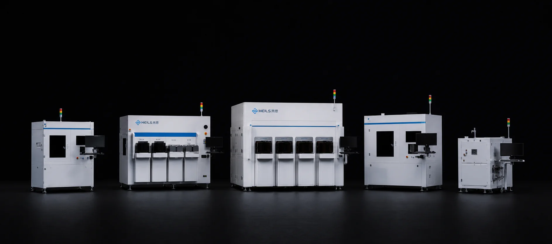
Advanced Ceramic Components
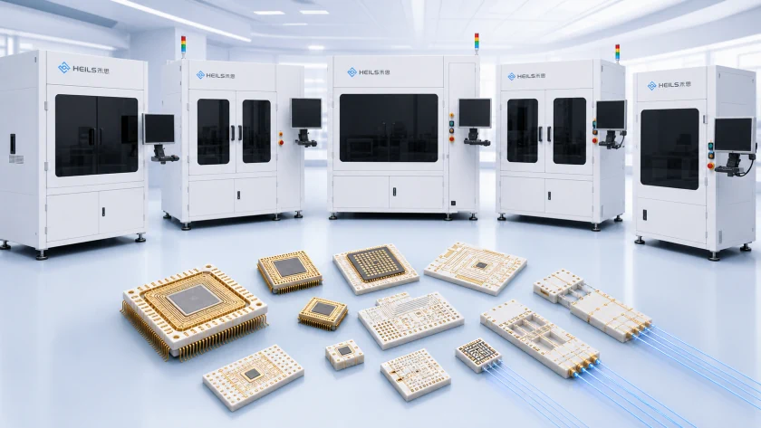
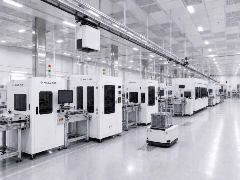
Focused on semiconductor ceramic devices, the solution covers full-site testing, inspection, sorting, and repair to improve chip reliability.
Vision Inspection
TKF500 Glass Substrate Surface Inspection System
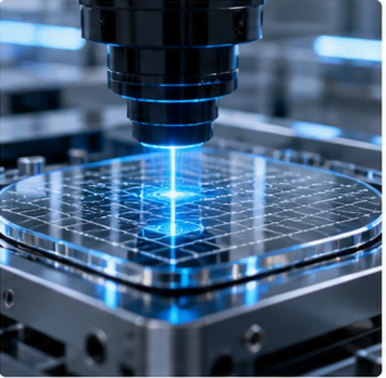
The TKF500 Glass Substrate Surface Inspection System is designed for high-precision visual inspection, capable of rapid full inspection of numerous micro-holes in a single pass with an accuracy of ±5 μm. It is suitable for surface defect and dimensional measurement of glass and advanced ceramic components.
Product Advantages
High-Speed Multi-Hole Simultaneous Inspection:Utilizes parallel optical imaging and a high-speed scanning mechanism to fully inspect hundreds of micro-holes in a single scan, significantly increasing production throughput.
Micron-Level Measurement Accuracy:Inspection accuracy is strictly controlled at ±5 μm, meeting the high-standard dimensional measurement requirements of semiconductor packaging and advanced ceramics.
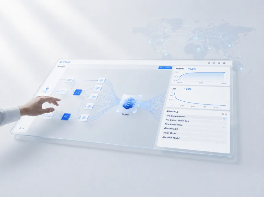
Intelligent Defect Recognition:Integrates deep learning algorithms to accurately identify subtle defects such as cracks, chipping, and hole wall roughness, reducing false rejection rates.
Flexible Substrate Compatibility:Accommodates glass and ceramic substrates of various sizes and thicknesses, enabling quick changeover for multi-variety production requirements.
Integrated Data Management:Automatically generates inspection reports and SPC statistics, supports MES integration, and enables quality traceability throughout the production process.
Product Functions
Product Specifications
- Inspection Accuracy:
- ±5 μm
- Inspection Speed:
- ≥500 mm²/sTypical value, may vary slightly with substrate complexity
- Max Substrate Size:
- Up to 500 mm × 500 mmCustomizable for larger sizes
- Min Detectable Hole Diameter:
- 10 μmDepends on optical system configuration
- Vision System:
- High-magnification dual-telecentric lens + high-resolution industrial camera
- Equipment Dimensions:
- Approx. 2000 mm × 1500 mm × 1800 mmIncludes loading/unloading module
Applications
Display Panel Glass Substrates:Inspects through-holes and blind vias on TFT-LCD and OLED substrates for dimensional accuracy and edge defects, ensuring pixel-level reliability.
Semiconductor Package Substrates:Performs comprehensive inspection of micro-hole arrays on IC carriers and interposers, ensuring consistency of conductive vias.
Advanced Ceramic Components:Suitable for surface quality and micro-hole parameter inspection of ceramic package bases, filters, and resonators.
Precision Screens and Molds:Inspects aperture area and shape errors of high-density screens, as well as hole position accuracy of precision molds.