
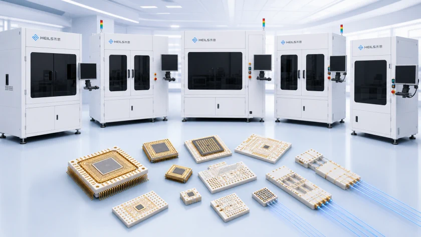



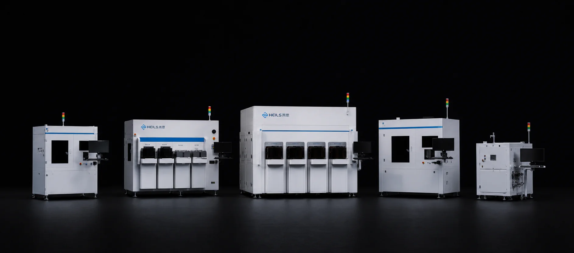
Advanced Ceramic Components
Focused on semiconductor ceramic devices, the solution covers full-site testing, inspection, sorting, and repair to improve chip reliability.

Vision Inspection
HS-F3000 SMT Inspection System
This system is a high-precision vision inspection solution designed specifically for solder paste printing quality inspection before SMT placement. Utilizing advanced optical imaging and intelligent algorithms, it precisely measures critical parameters such as solder paste height, area, volume, and offset to ensure soldering reliability.
Product Advantages
High-Precision 3D Measurement:Employs multi-angle structured light projection technology to accurately reconstruct the 3D topography of solder paste with micron-level repeatability.
Intelligent Defect Recognition:Integrates deep learning algorithms to automatically identify common defects such as insufficient solder, excess solder, bridging, peaks, and offset, reducing false alarm rates.
High-Speed Inline Inspection:Supports high-speed line integration with short inspection cycles, meeting the throughput demands of mass production.
Flexible Programming:Adaptable to various PCB form factors and solder paste processes, enabling quick setup of inspection programs and short changeover times.
Full Process Data Traceability:Real-time recording of inspection data and images generates statistical reports for easy process analysis and quality traceability.
Product Functions
Product Specifications
- X/Y Resolution:
- 10 μmCustomizable for higher precision
- Inspection Items:
- Height, area, volume, offset, bridging, etc.
- Field of View:
- 50mm×50mmOther specifications available
- Inspection Speed:
- 0.5 sec/FOVDepends on configuration
- PCB Size Range:
- 50mm×50mm ~ 510mm×460mmExpandable upon request
- Lighting System:
- Multi-angle structured light + RGB ring lightCustom optical solutions
Applications
Smartphone Motherboard Manufacturing:Inspects solder paste on high-density 0201 components and BGA pads, ensuring yield in miniaturized packaging.
Automotive Electronic Control Units:Ensures consistent solder paste printing on large PCBs and thick copper boards, meeting automotive-grade reliability requirements.
Semiconductor Package Substrates:Used for fine-pitch solder paste inspection on advanced packaging substrates such as FC-BGA, controlling micro-bump defects.
Consumer Electronics Module Assembly:Meets the solder paste quality monitoring needs for precision components like camera modules and connectors.